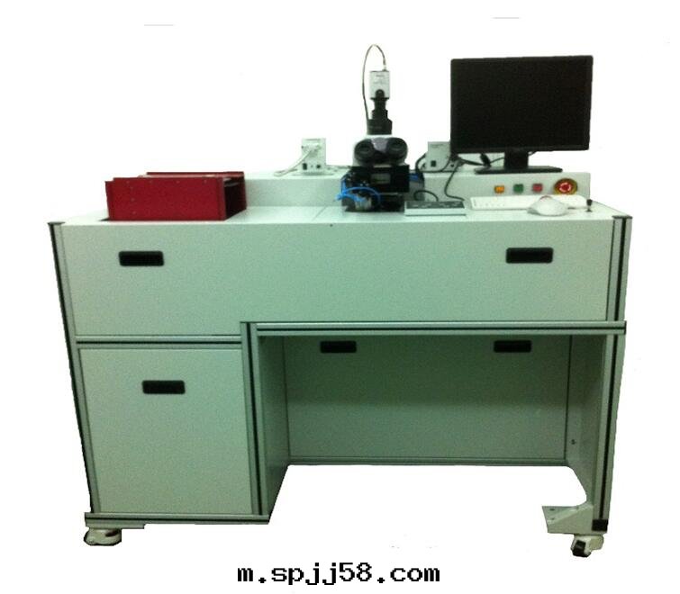
Sawn Wafer Inspection System SI-Series
with wafer mapping E142 compatible to Olympus microscope systems
Benefits
 Seamless integrate with Olympus MX-series and BXFM microscope systems
 Programmable motorised stage to handle wafer ring size up to 16” or 440 mm
 Auto-loader for wafer ring cassette (eliminate handling direct to wafer / product)
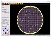
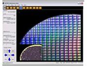
 Graphical and GUI electronic wafer map or bin code map configuration
 RFID for cassette ID registration and automatic wafer ID reader
 SEMI E142 compliant wafer mapping structure
 SECS/GEMS E142 SECS II compliant communication
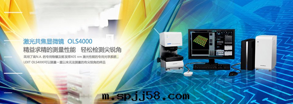
——无锡(xī)世邁科技检測系统解(jiě)決方(fāng)案(àn)——
无锡(xī)世邁科技为(wèi)您提(tí)供奧林(lín)巴斯工業显微鏡(jìng)設備及(jí)配件(jiàn),适應(yìng)新(xīn)産品、新(xīn)工藝需求的(de)設備。
热(rè)線(xiàn)电話(huà):13601489565
官网(wǎng)网(wǎng)址:http://m.spjj58.com
邮(yóu)箱(xiāng):sally_sheng@m.spjj58.com